DeepTech & Manufacturing
August 8, 2025

From Years to Days: How AI is Redefining Chip Design

This is the first piece of a new series exploring how AI is reshaping the physical world, one industry at a time.

What happens when the two of the most valuable “chip” companies don’t make chips at all? Synopsys and Cadence each now trade above Intel’s market cap — proof that design software, not fabs, is silicon’s deepest moat.

Yet that moat is cracking.

After decades of slow, manual workflows, chip design is finally getting its AWS + Github moment, powered by AI. What once took hundreds of engineers and over a year can now be done in days with AI tools that can generate layouts, catch bugs, and even write RTL code.

The semiconductor industry, long considered unshakeable, is entering a new era of AI-native tooling, and the shift is already underway.

From Mylar Sheets to Oligopoly

In the 1970s, chip design was a painstaking craft. Engineers literally drew circuits on Mylar sheets. Verification was done manually, designs were reviewed line by line.

As chips grew more complex, so did the need for the tools needed to build them. Then Electronic Design Automation (EDA) took over moving design to software, where logic became code and simulations replaced hand checks.

Fun fact: The first microprocessor, Intel 4004, was hand-drawn with 2,300 transistors. Today’s chips, like Apple’s M2 Ultra, have over 134 billion transistors. That is a 58 million× leap in complexity.
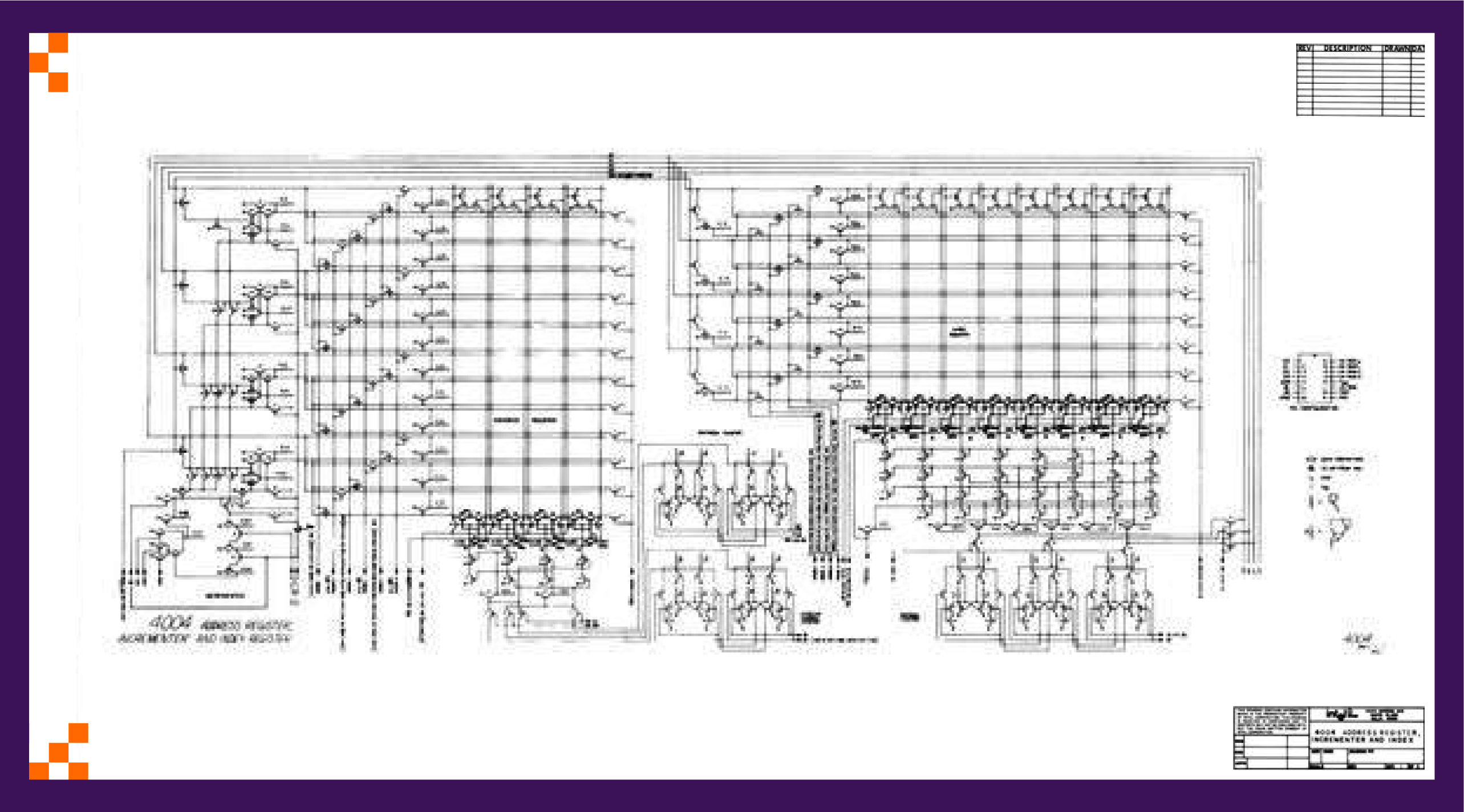
This electrical circuit schematic shows how the 2,300 transistors of the Intel 4004 microprocessor are interconnected. (Source: Computer History Museum)

By the 1990s, Synopsys, Cadence, and Mentor Graphics (later Siemens) consolidated their dominance; today they are responsible for over 70% of EDA sales.

Magma IPO’d in 2001, only to be acquired by Synopsys, a decade later. Dozens of upstarts tried to break through. Most met one of two fates: acquisition or failure.

So, why are there so few winners? Here’s our take:

  • Risk aversion: One design error can ruin a $100M tapeout.
  • Fab lock-in: Top foundries like TSMC have tight partnerships with the "big three" EDA vendors and certify only a few toolchains. More on this here.
  • Relationship-driven sales: Tool adoption is about trust as much as tech.

AI won’t magically erase these barriers. But it can find cracks in the wall.

Why Now?

So why is AI finally shaking up chip design after decades of stasis? Three shifts collided:

  1. Making chips is now easy:

A decade ago, only giants like Intel, NVIDIA, and AMD could make chips. Today, with increased compute requirements, AI-hungry startups are building custom silicon for AI workloads. But they can’t afford $50K‑a‑seat EDA tools or 3‑year design cycles.

By 2030, AI-focused chips will power most servers. (Source: McKinsey Estimates)

2. Old processes can’t keep up

Design productivity has not kept up with chip complexity: SoCs now pack billions of elements. Verification is slow, manual and hit-and-trial. When time-to-market is king, any tool that cuts weeks or months off the design cycle will win.

3. The industry is faced with a global talent shortage

According to this Forbes piece, the semiconductor industry will need 1 million additional skilled workers by 2030. Fewer students, an ageing workforce, and rising chip demand are only increasing the gap. AI can reduce the designer-to-verification-engineer ratio from 1:6 to 1:1.

As NVIDIA’s CEO, Jensen Huang put it: “The future of chip design is one human surrounded by hundreds of AIs.”
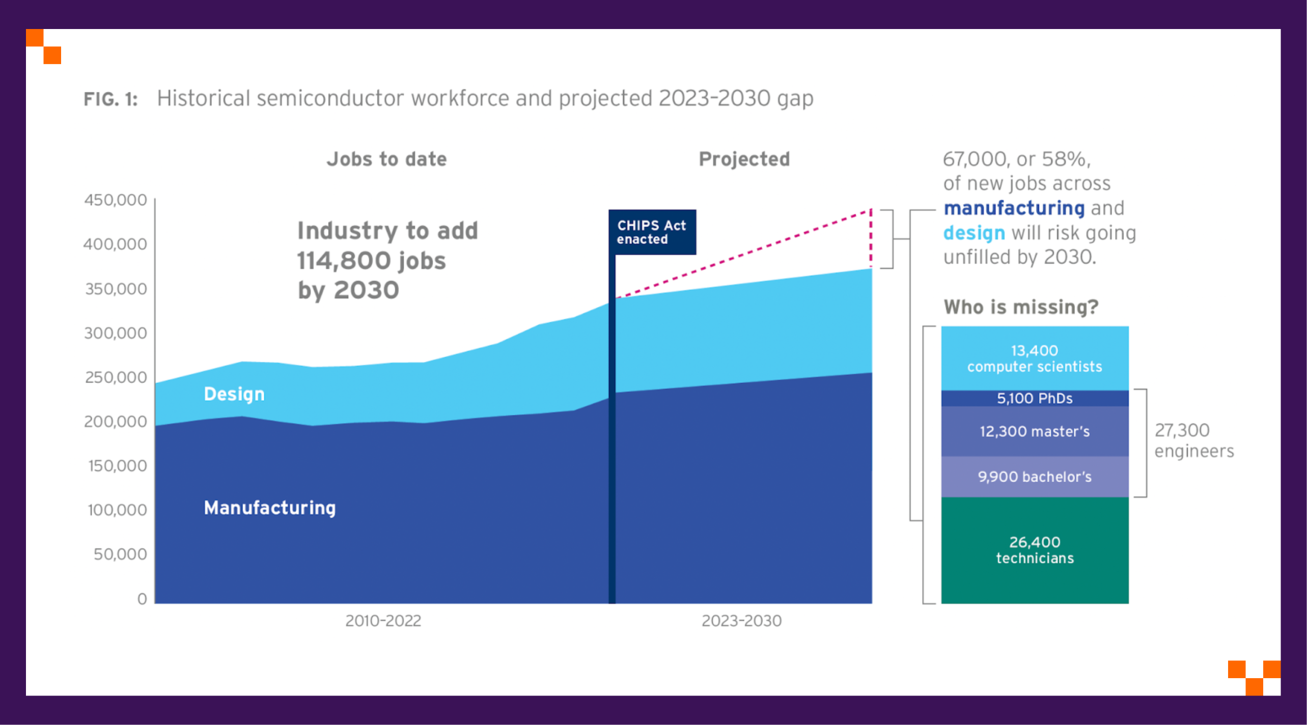
The Semiconductor Talent Crunch Is Real: 67K design & manufacturing roles may remain vacant by 2030. (Source: Semiconductor Industry Association)

How can AI solve these bottlenecks?

Finding better designs, faster
AI can explore billions of possible configurations far beyond human capacity. Synopsys’ DSO.ai runs thousands of simulations to improve PPA (power, performance, area), cutting timelines by months.

Learning from iterationGoogle DeepMind’s AlphaChip used reinforcement learning to floorplan chips in under six hours, outperforming humans on wire length and layout efficiency. This is a big deal, suggesting we’re nearing an era of AI-autonomous physical design.
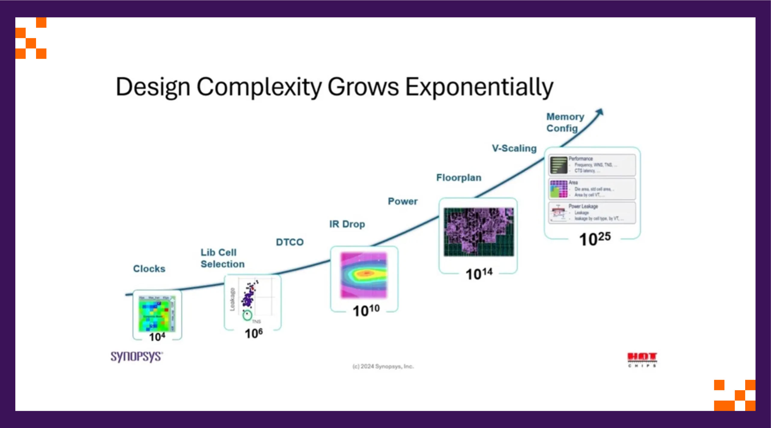
Design complexity increases the need for AI-enhanced tools. Source : Semiconductor Engineering

GenAI as an assistant
Cadence’s ChipGPT can interpret specs, generate HDL code, and suggest fixes, freeing engineers for higher‑level decisions. While useful for productivity, it’s not yet proven for creative, from‑scratch HDL generation.

Where the opportunity lies

While the incumbents continue to evolve their tools, startups may be better positioned to take bold, focused bets on how AI can reshape chip design from the ground up.

By breaking down the chip design cycle, we can identify the key areas where startups are driving innovation:
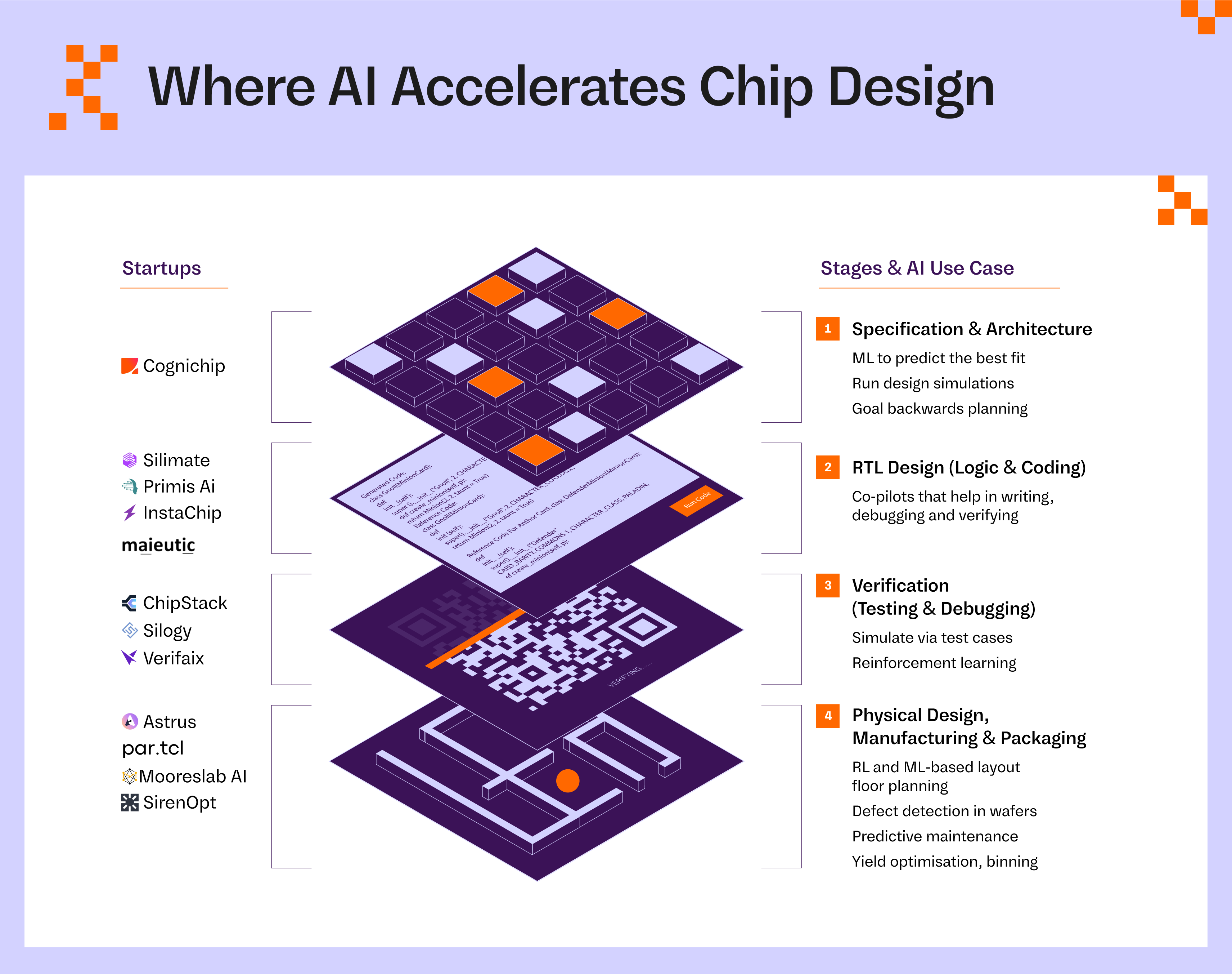
1. Specification & Architecture

This is the idea stage: defining what the chip should do, which processing units it needs, memory size, and special features. AI can act as a smart assistant, exploring different architecture options much faster than a human.

  • Cognichip is building what it calls “Artificial Chip Intelligence (ACI)”, a foundation AI model for chips. They raised $33 M seed round led by Lux Capital and Mayfield. The founder, Faraj Aalaei (who has taken two chip companies public), says his vision is to cut development time by 50% and costs by 75% using AI.

Our View
This is a promising area for companies building chips from scratch or working on completely new designs. However, large semiconductor companies typically build on top of well-established architecture families, limiting the need for new design exploration.

2. RTL Design (Logic & Coding)

The architecture becomes code in hardware description languages like Verilog or VHDL. It’s a painstaking process, often involving millions of lines of code and endless reviews to catch bugs.

The RTL design stage has seen the most startup activity, with multiple young companies building AI-driven design tools:

  • ChipStack uses LLMs to suggest code as the designer types, auto-complete the wiring of signals, and generate test benches for verification.

  • Silimate is building an AI assistant that can find functional bugs in the design and performance violations. They recently brought on Tenstorrent as a customer.

  • Maieutic Semiconductor, an Indian deep-tech startup, is building an AI copilot specifically for analog chip design which is still a 75% manual process. They recently raised a $4.15 M seed round co-led by Endiya Partners and Exfinity Venture Partners.

Our View
We believe front-end design will remain human-led as Generic RTL copilots are already robust. The opportunity is in context‑aware AI that understands the chip’s constraints and design goals.

3. Verification (Testing & Debugging)

After and during the design coding, verification engineers write and run tests to check every aspect of the chip’s logic against the specifications. This is heaviest lift in chip design: ~70% of total effort and highly repetitive. AI can help simulate and test all the important scenarios, often missed by traditional coverage metrics

  • Silogy’s AI agent “Viv” can diagnose the root cause of test failures in minutes, helping bring new chips to market up to 10× faster.

  • Verifaix is building AI agents for spec analysis, testplan/testbench generation, and debug, automating various parts of the verification flow.

Our View
The most promising wedge: Verification workflows command nearly 70% of design effort, are standardised, data-rich and painful, therefore ripe for automation. If an AI tool can truly improve test coverage, detect errors earlier, and speed up debugging, companies will be eager to adopt it as an additional layer on top of their existing workflows.

4. Physical Design, Manufacturing and Packaging

At this stage, the chip moves from logic to physical reality, converting code into a geometric layout of transistors and wires through place-and-route. AI, especially reinforcement learning, can optimise this layout for Power, Performance, and Area (PPA) far faster than human engineers.

Once the design is finalised, it's sent to fabs (like TSMC) for manufacturing, where AI helps spot defects early using sensor and test data. Finally, during packaging, AI assists in planning multi-die layouts, predicting heat/stress risks, and routing complex inter-chip connections.

  • Astrus automates analog layouts to instantly generate a workable transistor layout, compressing timelines by months. Founded in 2022, Astrus raised a $2.4 M pre-seed led by Khosla Ventures in 2023.

  • SirenOpt is building an AI-powered quality control platform. Using their novel sensor technology plus machine learning, they can monitor material properties in real time on production lines, detecting subtle variations or defects that traditional tests miss.

Our View
This layer is hard to build for, but if cracked, it offers deep moats and sticky customers.

  • Using AI for physical design is real, where companies like Google have published papers showing RL-based floorplanning outperforming human results. Startups here must show clear PPA wins to succeed.

  • Manufacturing AI depends on tight fab integration and data access, which is a tough moat to break for new entrants unless they partner with a foundry or EDA giant.

  • Packaging AI is still emerging, but growing in importance with multi-die architectures becoming mainstream. Tools that can help model and optimise 3D chiplets and thermal flows have a clear edge.

Watch-outs for founders

Here are the key things that a founder starting in this space should think about:

  1. Don’t build what generic LLMs will soon match
    Over time, general-purpose LLMs will ingest similar data and close the gap. Founders should focus on chip-specific workflows or agents that generic LLMs cannot easily replicate. The co-pilot universe is increasingly becoming a winner-takes-all market.

  2. Avoid going head on against EDA giants
    Instead, find a narrow wedge: a use case or workflow where EDA tools are weak or slow-moving, and build on top of the existing ecosystem. Bring them in as early partners, not adversaries.

  3. Co-design with 2–3 anchor customers
    This is not a “build in isolation and launch” kind of market. Semiconductor teams have highly specific needs, and success requires a customer-centric approach. Founders should partner with a few deep-tech teams early on and co-develop the solution with real users.

  4. Ship fast with the right team
    The space is highly dynamic, so show real results, fast. Build a team around deep EDA domain knowledge and AI expertise, and bridge the two worlds.

Summing Up

AI for chip design isn’t “push a button, get a chip.” It’s re-engineering the loop between idea and output, collapsing months into weeks, freeing engineers from drudgery, and embedding intelligence into every step of the process.

By 2035, designing a chip should be no harder than building any other hardware product. The architecture will be sketched out on a napkin. A three-person team drafts specs on a whiteboard. An AI assistant compiles, verifies and simulates the design in hours. The foundry tapeout process gets significantly streamlined. The whole process takes a few months — a process that once took years.

This isn't a theory. AI is already inside chip teams at Nvidia, AMD, and every ambitious startup. Billions in funding are flowing into AI-EDA.

Founders, engineers, skeptics: what do you see coming next?

Where will AI crack the cycle first?

Will verification be the wedge, or will another stage break open sooner?

Will the big three out-build, or just out-buy, the next wave?

At Z47, we invest in dev tools for the physical world: semiconductors, aerospace, energy, manufacturing, and robotics. If you’re building in this space, write to us at physical.ai@z47.com.

For more information, write to us: namaste@Z47.com.
Stay connected with Z47.

Watch more such podcasts

DeepTech & Manufacturing
December 12, 2025

India’s Blueprint for Deep Tech Leadership: Insights from DMII 3.0

DeepTech & Manufacturing
September 12, 2025

Hand-routed to Co-piloted: When the nervous system of electronics meets AI

DeepTech & Manufacturing
February 15, 2024

The Digitizing Make in India Summit 2.0

DeepTech & Manufacturing
August 8, 2025

From Years to Days: How AI is Redefining Chip Design

Article
Listen to article

This is the first piece of a new series exploring how AI is reshaping the physical world, one industry at a time.

What happens when the two of the most valuable “chip” companies don’t make chips at all? Synopsys and Cadence each now trade above Intel’s market cap — proof that design software, not fabs, is silicon’s deepest moat.

Yet that moat is cracking.

After decades of slow, manual workflows, chip design is finally getting its AWS + Github moment, powered by AI. What once took hundreds of engineers and over a year can now be done in days with AI tools that can generate layouts, catch bugs, and even write RTL code.

The semiconductor industry, long considered unshakeable, is entering a new era of AI-native tooling, and the shift is already underway.

From Mylar Sheets to Oligopoly

In the 1970s, chip design was a painstaking craft. Engineers literally drew circuits on Mylar sheets. Verification was done manually, designs were reviewed line by line.

As chips grew more complex, so did the need for the tools needed to build them. Then Electronic Design Automation (EDA) took over moving design to software, where logic became code and simulations replaced hand checks.

Fun fact: The first microprocessor, Intel 4004, was hand-drawn with 2,300 transistors. Today’s chips, like Apple’s M2 Ultra, have over 134 billion transistors. That is a 58 million× leap in complexity.

This electrical circuit schematic shows how the 2,300 transistors of the Intel 4004 microprocessor are interconnected. (Source: Computer History Museum)

By the 1990s, Synopsys, Cadence, and Mentor Graphics (later Siemens) consolidated their dominance; today they are responsible for over 70% of EDA sales.

Magma IPO’d in 2001, only to be acquired by Synopsys, a decade later. Dozens of upstarts tried to break through. Most met one of two fates: acquisition or failure.

So, why are there so few winners? Here’s our take:

  • Risk aversion: One design error can ruin a $100M tapeout.
  • Fab lock-in: Top foundries like TSMC have tight partnerships with the "big three" EDA vendors and certify only a few toolchains. More on this here.
  • Relationship-driven sales: Tool adoption is about trust as much as tech.

AI won’t magically erase these barriers. But it can find cracks in the wall.

Why Now?

So why is AI finally shaking up chip design after decades of stasis? Three shifts collided:

  1. Making chips is now easy:

A decade ago, only giants like Intel, NVIDIA, and AMD could make chips. Today, with increased compute requirements, AI-hungry startups are building custom silicon for AI workloads. But they can’t afford $50K‑a‑seat EDA tools or 3‑year design cycles.

By 2030, AI-focused chips will power most servers. (Source: McKinsey Estimates)

2. Old processes can’t keep up

Design productivity has not kept up with chip complexity: SoCs now pack billions of elements. Verification is slow, manual and hit-and-trial. When time-to-market is king, any tool that cuts weeks or months off the design cycle will win.

3. The industry is faced with a global talent shortage

According to this Forbes piece, the semiconductor industry will need 1 million additional skilled workers by 2030. Fewer students, an ageing workforce, and rising chip demand are only increasing the gap. AI can reduce the designer-to-verification-engineer ratio from 1:6 to 1:1.

As NVIDIA’s CEO, Jensen Huang put it: “The future of chip design is one human surrounded by hundreds of AIs.”

The Semiconductor Talent Crunch Is Real: 67K design & manufacturing roles may remain vacant by 2030. (Source: Semiconductor Industry Association)

How can AI solve these bottlenecks?

Finding better designs, faster
AI can explore billions of possible configurations far beyond human capacity. Synopsys’ DSO.ai runs thousands of simulations to improve PPA (power, performance, area), cutting timelines by months.

Learning from iterationGoogle DeepMind’s AlphaChip used reinforcement learning to floorplan chips in under six hours, outperforming humans on wire length and layout efficiency. This is a big deal, suggesting we’re nearing an era of AI-autonomous physical design.

Design complexity increases the need for AI-enhanced tools. Source : Semiconductor Engineering

GenAI as an assistant
Cadence’s ChipGPT can interpret specs, generate HDL code, and suggest fixes, freeing engineers for higher‑level decisions. While useful for productivity, it’s not yet proven for creative, from‑scratch HDL generation.

Where the opportunity lies

While the incumbents continue to evolve their tools, startups may be better positioned to take bold, focused bets on how AI can reshape chip design from the ground up.

By breaking down the chip design cycle, we can identify the key areas where startups are driving innovation:

1. Specification & Architecture

This is the idea stage: defining what the chip should do, which processing units it needs, memory size, and special features. AI can act as a smart assistant, exploring different architecture options much faster than a human.

  • Cognichip is building what it calls “Artificial Chip Intelligence (ACI)”, a foundation AI model for chips. They raised $33 M seed round led by Lux Capital and Mayfield. The founder, Faraj Aalaei (who has taken two chip companies public), says his vision is to cut development time by 50% and costs by 75% using AI.

Our View
This is a promising area for companies building chips from scratch or working on completely new designs. However, large semiconductor companies typically build on top of well-established architecture families, limiting the need for new design exploration.

2. RTL Design (Logic & Coding)

The architecture becomes code in hardware description languages like Verilog or VHDL. It’s a painstaking process, often involving millions of lines of code and endless reviews to catch bugs.

The RTL design stage has seen the most startup activity, with multiple young companies building AI-driven design tools:

  • ChipStack uses LLMs to suggest code as the designer types, auto-complete the wiring of signals, and generate test benches for verification.

  • Silimate is building an AI assistant that can find functional bugs in the design and performance violations. They recently brought on Tenstorrent as a customer.

  • Maieutic Semiconductor, an Indian deep-tech startup, is building an AI copilot specifically for analog chip design which is still a 75% manual process. They recently raised a $4.15 M seed round co-led by Endiya Partners and Exfinity Venture Partners.

Our View
We believe front-end design will remain human-led as Generic RTL copilots are already robust. The opportunity is in context‑aware AI that understands the chip’s constraints and design goals.

3. Verification (Testing & Debugging)

After and during the design coding, verification engineers write and run tests to check every aspect of the chip’s logic against the specifications. This is heaviest lift in chip design: ~70% of total effort and highly repetitive. AI can help simulate and test all the important scenarios, often missed by traditional coverage metrics

  • Silogy’s AI agent “Viv” can diagnose the root cause of test failures in minutes, helping bring new chips to market up to 10× faster.

  • Verifaix is building AI agents for spec analysis, testplan/testbench generation, and debug, automating various parts of the verification flow.

Our View
The most promising wedge: Verification workflows command nearly 70% of design effort, are standardised, data-rich and painful, therefore ripe for automation. If an AI tool can truly improve test coverage, detect errors earlier, and speed up debugging, companies will be eager to adopt it as an additional layer on top of their existing workflows.

4. Physical Design, Manufacturing and Packaging

At this stage, the chip moves from logic to physical reality, converting code into a geometric layout of transistors and wires through place-and-route. AI, especially reinforcement learning, can optimise this layout for Power, Performance, and Area (PPA) far faster than human engineers.

Once the design is finalised, it's sent to fabs (like TSMC) for manufacturing, where AI helps spot defects early using sensor and test data. Finally, during packaging, AI assists in planning multi-die layouts, predicting heat/stress risks, and routing complex inter-chip connections.

  • Astrus automates analog layouts to instantly generate a workable transistor layout, compressing timelines by months. Founded in 2022, Astrus raised a $2.4 M pre-seed led by Khosla Ventures in 2023.

  • SirenOpt is building an AI-powered quality control platform. Using their novel sensor technology plus machine learning, they can monitor material properties in real time on production lines, detecting subtle variations or defects that traditional tests miss.

Our View
This layer is hard to build for, but if cracked, it offers deep moats and sticky customers.

  • Using AI for physical design is real, where companies like Google have published papers showing RL-based floorplanning outperforming human results. Startups here must show clear PPA wins to succeed.

  • Manufacturing AI depends on tight fab integration and data access, which is a tough moat to break for new entrants unless they partner with a foundry or EDA giant.

  • Packaging AI is still emerging, but growing in importance with multi-die architectures becoming mainstream. Tools that can help model and optimise 3D chiplets and thermal flows have a clear edge.

Watch-outs for founders

Here are the key things that a founder starting in this space should think about:

  1. Don’t build what generic LLMs will soon match
    Over time, general-purpose LLMs will ingest similar data and close the gap. Founders should focus on chip-specific workflows or agents that generic LLMs cannot easily replicate. The co-pilot universe is increasingly becoming a winner-takes-all market.

  2. Avoid going head on against EDA giants
    Instead, find a narrow wedge: a use case or workflow where EDA tools are weak or slow-moving, and build on top of the existing ecosystem. Bring them in as early partners, not adversaries.

  3. Co-design with 2–3 anchor customers
    This is not a “build in isolation and launch” kind of market. Semiconductor teams have highly specific needs, and success requires a customer-centric approach. Founders should partner with a few deep-tech teams early on and co-develop the solution with real users.

  4. Ship fast with the right team
    The space is highly dynamic, so show real results, fast. Build a team around deep EDA domain knowledge and AI expertise, and bridge the two worlds.

Summing Up

AI for chip design isn’t “push a button, get a chip.” It’s re-engineering the loop between idea and output, collapsing months into weeks, freeing engineers from drudgery, and embedding intelligence into every step of the process.

By 2035, designing a chip should be no harder than building any other hardware product. The architecture will be sketched out on a napkin. A three-person team drafts specs on a whiteboard. An AI assistant compiles, verifies and simulates the design in hours. The foundry tapeout process gets significantly streamlined. The whole process takes a few months — a process that once took years.

This isn't a theory. AI is already inside chip teams at Nvidia, AMD, and every ambitious startup. Billions in funding are flowing into AI-EDA.

Founders, engineers, skeptics: what do you see coming next?

Where will AI crack the cycle first?

Will verification be the wedge, or will another stage break open sooner?

Will the big three out-build, or just out-buy, the next wave?

At Z47, we invest in dev tools for the physical world: semiconductors, aerospace, energy, manufacturing, and robotics. If you’re building in this space, write to us at physical.ai@z47.com.

We are excited about the innovation and growth opportunities in this sector.

If you are considering building in the footwear space, we’d love to chat.
Drop us a line at consumer@matrixpartners.in

Learnt something new? Follow us!

Vs NIFTY 500
+9.1%
Since Jan 2024
USD/INR
₹95.19
▲ +0.6%
Daily change • 1 Ju1 2025
128.1
▲ +28.1%
Since Jan 2024
NIFTY 500
129.1
▲ +19.0%
Since Jan 2024

Index Performance

+28.1%
Since Jan 2024
NIFTY 500
+19.0%
Since Jan 2024

Z47^fortyseven is up +23.9% since its January 2024 base date, versus Nifty 500's +18.4%, ahead by 550 bps.

The cohort moved +4.7% over the month versus Nifty 500's +2.5%, leading by 220 bps.

Anchored in domestic demand and rising digital adoption, the cohort remained resilient amid global headwinds.

Consumer Tech was the best-performing sector at +9.2% last month, driven by sustained growth in consumer demand and strength in consumer-internet platforms.

Largest Constituents  ·  The Names That Anchor The Index

1.
Eternal
Quick-commerce leadership and continued investment
▲ +12.8%
2.
Groww
Broking market-share gains and margin-funding growth.
▲ +10.4%
3.
Lenskart
Store densification and margin expansion.
▲ +2.4%

Top Gainers  ·  Key Drivers

1 MONTH RETURN
1.
CarTrade
Auto-marketplace dominance and a cash-rich balance sheet.
▲ +59.4%
2.
 Amagi Media Labs
Profitability turnaround and AI-led cloud media adoption.
▲ +31.4%

Top Laggards  ·  Key Drivers

1 MONTH RETURN
1.
Fractal Analytics
Enterprise AI spending trends and post-listing share supply.
▼ -10.8%
2.
MedPlus Health
Pharmacy-margin pressure and competitive intensity.
▼ -6.6%

Key Themes  ·  Latest Results

In Q4FY26, Z47^fortyseven's cohort grew top line ~39% YoY, more than 3x the broad market's ~12% growth.

Operating leverage lifted net margins around 500 bps into positive territory, even as broad-market net margins remained roughly flat.

With 40 of 47 companies now profitable, the cohort reflects a broader shift toward profitable growth over growth at any cost.

AI adoption runs deeper across this cohort than in the broader market, with companies using it to drive growth and reshape demand, not just improve efficiency.

Cash generation is increasingly defining the winners, enabling market leaders like Eternal, CarTrade, and PB Fintech to fund acquisitions and expansion from their own balance sheets.

Market & Macro Context

The cohort saw several block deals this month, including sizeable stake sales in Lenskart, Delhivery, Honasa, and Shadowfax.

Ownership continues to shift from foreign investors to domestic institutions, creating a more durable shareholder base.

AI remained the defining technology investment theme, driving capital deployment across both private and public markets.

IPO Takeaway · Kissht

Listed May 2026

A modest listing pop followed by strong post-listing gains reinforced the market's preference for asset quality and disciplined underwriting over pure loan-book growth.

The listing helped reset perceptions around unsecured lending, creating a constructive valuation anchor for the issuers that follow.

The buyer mix was a notable positive — strong participation from long-only domestic institutions supporting a durable post-listing ownership base.

Net Read

Fundamentals continued to strengthen across the cohort, with growth, margins, and cash generation improving in tandem.

Performance dispersion widened, with profitability and earnings quality increasingly distinguishing the strongest performers from the rest.

Disclaimer

Z47^fortyseven is published for informational purposes only and does not constitute investment advice, or any offer, solicitation, or recommendation to buy or sell securities. Index performance is historical and should not be construed as indicative of future results.

Explore the live index
Read Previous Article On Land & Expand
Read Next Article On Land & Expand