

This is the second in our series on how AI is reshaping the physical world: we now turn our attention to printed circuit boards (PCBs). For the Z47 perspective on AI in Chips, go here.
From smartphones to EVs, from toasters to satellites, there’s a silent workhorse that powers them all. We’re talking about the printed circuit board (PCB).
These green (or blue) slabs tie chips, power, and signals together, forming the foundation of modern technology. Chips do the computing; PCBs connect power and signals so products actually work.
In our last article, we showcased how AI is compressing chip design timelines from years to days. The same shift is arriving in PCB design: a field that still relies on manual placement, hand-routing, and long review cycles. This piece maps where AI is landing, why now, and what founders are building.
Why do PCBs Matter?
Every electronic product rests on a PCB. If semiconductors are the brain, PCBs are the nervous system: carrying power, signals, and instructions across the system. Without a board, chips are just isolated islands of silicon.
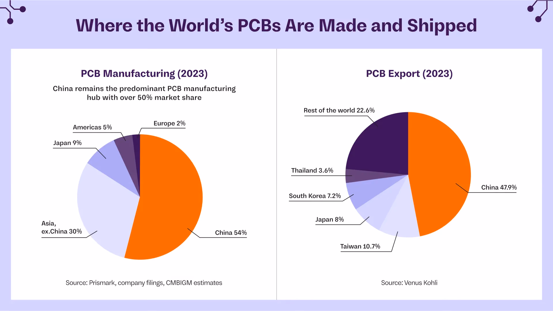
This invisible layer is also an $80B+ global industry. China, often called the “PCB Capital of the World” controls more than half of global manufacturing, thanks to decades of investment in fabrication capacity, supply chain depth in components, and low-cost labor. By 2030, the global PCB market is projected to cross $100B, with Asia (China, Taiwan, South Korea) continuing to dominate.
PCBs are not monolithic. They come in many flavors: rigid boards for laptops and servers, flexible PCBs for wearables and smartphones, and high-density interconnect (HDI) boards for compact, sensor-rich IoT devices. The complexity has risen with every new wave of technology.
Designing these boards is a painstaking process. Engineers must balance thousands of constraints:
- Electrical: impedance, crosstalk, signal integrity.
- Thermal: heat dissipation, airflow, copper balancing.
- Mechanical: size, flex, connectors, edge tolerances.
- Manufacturability: fab limits, panelization, assembly tolerances
While a few giants dominate the chip EDA world, the PCB tool landscape has been more fragmented, with long-time players like Altium, Cadence (Allegro), Siemens Mentor (Xpedition), standing out.
PCB design remains a massive labour-driven cost center. Engineers (with decades of experience) manually place parts, trace copper paths, and run repeated reviews. Of the $40–50B spent on design, the majority goes to human time, not software. This is what makes PCB design an enormous opportunity to unlock with AI.
Why now for PCB design?
Three forces are pushing PCB design to its own “Copilot moment”:
- A spike in complexity
The last decade has seen evolution in the tech that powers electronic devices, with the “smartification” of everything. Devices are becoming smaller and denser. IoT, wearables, and EVs have pushed PCBs into flex, rigid-flex, and ultra-dense HDI formats. While factories have automated fabrication, design has become the choke point. - A talent shortage
Globally, a shortage of expertise is emerging in deep hardware design. Many veteran PCB designers are retiring, and fewer young engineers have PCB layout expertise. This has led to product delays, ballooning costs, and rising competition for scarce expertise.
- Proof points already working
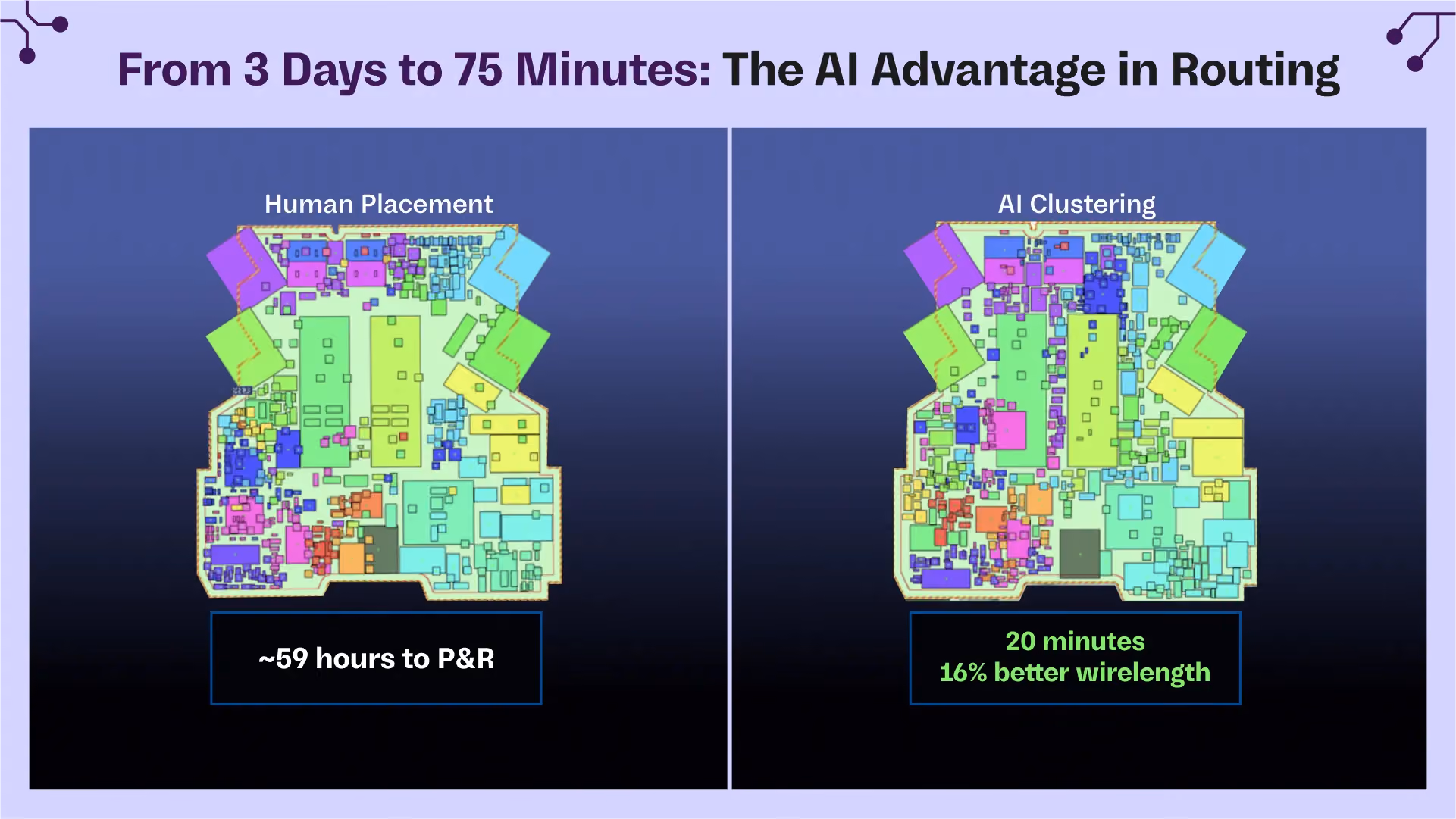
Perhaps the biggest reason for “why now” is that AI began showing results,even before the GPT era. Cadence’s Allegro X AI slashed routing from three days to 75 minutes, with higher quality. Open-source tools like KiCad and code-like formats such as Atopile and TS Circuits are breaking vendor lock-in and encouraging experimentation.
The technology inflection point is here. AI has finally matured to meet this challenge, and may arguably be better positioned than chips in some ways.
Where AI Is Entering the PCB Flow
AI isn’t replacing engineers outright, instead it’s targeting the slowest, most manual steps in the process.
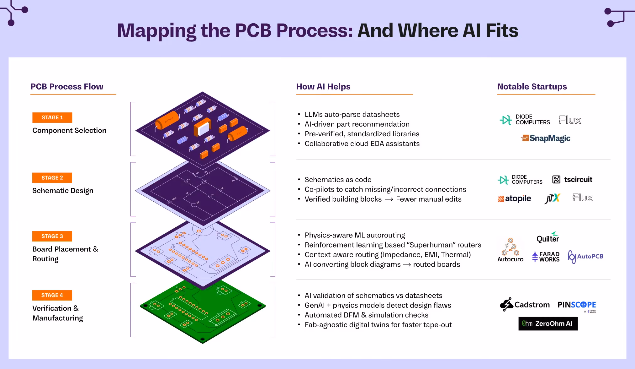
1. Component Selection & Schematic Design
Today, engineers slog through hundred-page datasheets, model parts in CAD tools, and draw schematics line by line. Getting it right is tough, there are thousands of components to choose from, and errors cascade downstream.
For decades, tools like Altium, Zuken and Eagle have dominated this stage. Their moat has been proprietary component libraries: verified collections of footprints, symbols, and supplier data. Altium even owns Octopart and Ciiva, two of the most popular electronic component search engines. But despite these advantages, the actual work of building schematics remains manual.
There have been attempts at change:
- KiCad gave startups and hobbyists an open-source alternative.
- Design platforms like Celus and Circuit Mind tried automating component selection and BOM generation.
- JITX and Flux experimented with code-first design: circuits were described in code, then compiled into schematics for further placement.
And now, AI is pushing it even further.
- Atopile has introduced an open, code-like format for schematics.
- Diode Computers uses LLMs to read datasheets and generate schematics as Atopile modules. Verified modules are added to its library, creating a compounding dataset that will eventually become its moat. Beyond schematics, Diode offerings extend into later stages of the PCB flow.
The opportunity here is clear: build standardized, trustworthy component libraries that engineers will adopt. In a field where mistakes cost weeks, trust is the product.
2. PCB Layout & DFM Optimization
This is the step that consumes half the design cycle. Engineers place components, route traces, and run endless checks for signal integrity, heat, and manufacturability.
Autorouters have been around since the 1980s. They could connect nets, but they didn’t understand design intent. Legacy autorouters couldn’t handle constraints like USB pairs needing matched lengths, so engineers still routed by hand.
Despite the presence of incumbents like Cadence Allegro, Mentor Xpedition (Siemens), most of the actual work is still manual.
Startups are going after the slowest, most painful part: routing.
- Quilter.ai calls itself a “compiler for PCBs.” Its physics-aware ML algorithms already cut routing time by 7x, and overall job time by 3.5x.
- Autocuro automates PCB design by reading system schematics and instantly placing and routing components, fully integrated with Altium, Cadence, and KiCad.
- Hence, the promise is not just connecting A to B, but embedding electrical, thermal, and fab constraints directly into the router.
Layout is the hardest nut to crack. Success depends on whether AI can capture the circuit context: not just wires, but the “why” behind them.
3. Manufacturing Integration & Verification
Once the layout is done, engineers export manufacturing files (Gerbers, BOMs, pick-and-place) and send them to a fab. Errors often show up only at this stage, after expensive prototypes.
Incumbents like Mentor Valor NPI and Cadence Sigrity dominate enterprise verification, while Altium 365 integrates fab checks into the cloud. But reviews are still manual, and simulations only catch so much.
AI is starting to help here too:
- Flux Copilot suggests fixes in real-time, like missing decoupling caps during the schematic layout.
- Cadstrom combines gen-AI with physics simulation to detect and resolve common PCB design issues automatically.
- PinScope (by FaradWorks) and ZeroOhm AI offer AI-driven PCB validation: designers upload files, AI checks them against datasheet rules, and flags critical errors before manufacturing.
The fragmentation of PCB manufacturing is actually an advantage here. Unlike chip design, there’s no TSMC. AI tools can build fab-agnostic pipelines, plugging directly into digital factories. The long-term vision: complex PCB design-to-delivery in under a week.
The Debate
However, the skepticism runs deep. Automation in PCB design has been tried before, and fallen short. The hesitation isn’t about speed, it’s about trust. PCB design is full of context-heavy decisions: impedance matching, thermal balancing, manufacturability rules. If an AI agent overlooks a constraint or misroutes a trace, who catches the mistake? And who takes responsibility?
AI has proven to be powerful but it is still not perfect.That’s why today’s tools aren’t sold as replacements, but as copilots. Engineers stay in the loop, reviewing and validating AI output while reaping massive time savings. Over time, confidence will grow, but only through repeated validation and proven results, not overnight promises.
Summing Up
AI is finally cracking open a space that has resisted change for decades. The playbook isn’t to reinvent everything, but to tackle the bottlenecks that consume human hours and stall product timelines.
The real moat in PCB design won’t be speed alone, it will be trust and adoption. Engineers will only switch when libraries are validated, models embed real-world constraints, and workflows fit seamlessly into existing tools. Founders who build that trust, layer by layer, will create defensible companies as enduring as the PCB incumbents of the last era.
For those building in this space, three execution aspects matter most:
- Trusted libraries of validated components.
- Context-rich models embedding electrical, thermal, and fab realities.
- Workflows engineers can actually adopt.
If they get this right, PCB design could shift from painful hand-routing to collaborative, Copilot-driven workflows as radical as Figma’s leap in software. China dominates manufacturing, but design is a global game, one where India’s software DNA and growing pool of hardware engineers can give it an edge. In a fragmented ecosystem with no “TSMC of PCBs,” the opportunity to build fab-agnostic, AI-native design platforms is wide open. The next breakout company in this space could just as easily be built from Delhi as from San Francisco.
.avif)
This isn't a theory anymore. Startups are building. Funding is flowing. The race is on.
At Z47, we invest in dev tools for the physical world: semiconductors, aerospace, energy, manufacturing, and robotics. If you’re building at the intersection of AI and PCB design, write to us at physical.ai@z47.com.
%20(1).avif)
%20(1).avif)


.webp)
.avif)
%20(1).avif)
.svg)


